Monday, February 8, 2010

Determining your Computer RAM Type

Type

  • FPM – Fast Page - If you have a 486, you probably have FPM

  • EDO – Extended Data Out - If you have an early Pentium system, you probably have EDO

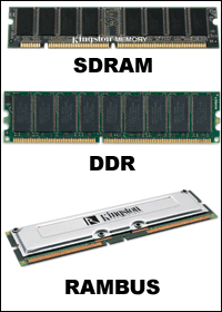
  • SDRAM - If you have a Pentium or Celeron system purchased in 1999, you probably have SDRAM

Sockets

Memory modules plug into a socket on the motherboard. There are three socket types.

  • SIMM30 pin – 3 inches in length

  • SIMM – 72 pin – 4 inches in length

  • DIMM168 pin – 5 inches in length

Most older 486 machines will use 30 pin modules. Later model 486 and Pentium machines will probably use 72 pin modules. More recent Pentium machines may have 168 pin.

Amount

Memory sizes increase by the power of 2. This results in sizes of 1, 2, 4, 8, 16, 32, 64, 128, 256 MBs.

  • On some older 486 machines, one memory module can be added at a time.

  • On most Pentium machines, modules must be added in pairs.

  • Each pair must be of the same size.

  • SDRAM modules can be added one at a time.

For example, if you have 8 MBs of memory on a Pentium, you have two 4 MB modules. To increase to 16 MBs, you need to add two more 4 MB modules. To increase to 24 MBs, you need to add two 8 MB modules.

Looking Inside

Now that you know the parameters, how do you determine which type you need? Looking inside the computer will not provide all of the information. It will confirm how many modules you currently have. You can also confirm the type and quantity of open sockets. If you only have four sockets and each socket contains a module, you will have to replace some of the existing memory modules.

Check the Manual

The other place to find the correct information is your owner’s manual. The manufacturer should have listed the type of memory required. You will need to determine the parity and speed.

Identification

Now that you have the necessary information, you find an ad for memory and still you may not be able to determine which modules you need. Why? Because the computer industry thrives on confusion and abbreviations. Here’s how to interpret the coding scheme.

30 pin modules

For 30 pin modules you will see something like

  • 1 x 9-60

  • 4 x 9-70

  • 4 x 8-70

The first number is the size in MB’s. In our example this would be 1MB or 4MB.

The second number represents parity. The value 9 represents parity and 8 represents non-parity. (Of course that makes a lot of sense!) The 9 or 8 also identifies that it is a 30 pin module.

The third value represents the speed.

72 pin modules

For 72 pin modules you will see something like

  • 1 x 32-60

  • 2 x 32-70

  • 4 x 36-60

  • 8 x 36-70

Just like the 30 pin modules, the first value represents the size, EXCEPT it only represents ¼ of the total memory size. Don’t ask why, just accept it. So the value of 4 represents a 16 MB (4 x 4) module. A value of 8 represents a 32 MB (4 x 8) module.

The second value, again just like the 30 pin, represents parity and the number of pins. 36 is used for parity and 32 for non-parity. You aren’t asking why again, are you?

The third value represents the speed, the same as the 30 pin

RAM Memory Technology

In order to enable computers to work faster, there are several types of memory available today. Within a single computer there is no longer just one type of memory. Because the types of memory relate to speed, it is important to understand the differences when comparing the components of a computer.

SIMM (Single In-line Memory Modules)
SIMMs are used to store a single row of DRAM, EDO or BEDO chips where the module is soldered onto a PCB. One SIMM can contain several chips. When you add more memory to a computer, most likely you are adding a SIMM.

The first SIMMs transferred 8 bits of data at a time & contained 30 pins. When CPU's began to read 32-bit chunks, a wider SIMM was developed & contained 72 pins.

72 pin SIMMS are 3/4" longer than 30 pin SIMMs & have a notch in the lower middle of the PCB. 72 pin SIMMs install at a slight angle.

DIMM (Dual In-line Memory Modules)
DIMMs allow the ability to have two rows of DRAM, EDO or BEDO chips. They are able to contain twice as much memory on the same size circuit board. DIMMs contain 168 pins & transfer data in 64 bit chunks.

DIMMs install straight up & down & have two notches on the bottom of the PCB.

SODIMM (Small Outline DIMM)
SO DIMMs are commonly used in notebooks & are smaller than normal DIMMs. There are two types of SO DIMMs. Either 72 pins and a transfer rate of 32 bits or 144 pins with a transfer rate of 64 bits.

RDRAM - RIMM
Rambus, Inc, in conjunction with Intel has created new technology, Direct RDRAM, to increase the access speed for memory. RIMMs appeared on motherboards sometime during 1999. The in-line memory modules are called RIMMs. They have 184 pins & provide 1.6 GB per second of peak bandwidth in 16 bit chunks. As chip speed gets faster, so does the access to memory & the amount of heat produced. An aluminum sheath, called a heat spreader, covers the module to protect the chips from overheating.

SO RIMM
Similar in appearance to a SODIMM & uses Rambus technology.

Technology

DRAM (Dynamic Random Access Memory)
One of the most common types of computer memory (RAM). It can only hold data for a short period of time & must be refreshed periodically. DRAMs are measured by storage capability & access time.

Storage is rated in megabytes (8 MB, 16 MB, etc).

Access time is rated in nanoseconds (60ns, 70ns, 80ns, etc) and represents the amount of time to save or return information. With a 60ns DRAM, it would require 60 billionths of a second to save or return information. The lower the nanospeed, the faster the memory operates.

DRAM chips require two CPU wait states for each execution.

Can only execute either a read or write operation at one time.

FPM (Fast Page Mode)
At one time, this was the most common & was often just referred to as DRAM. It offered faster access to data located within the same row.

EDO (Extended Data Out)
Newer than DRAM (1995) and requires only one CPU wait state. You can gain a 10 to 15% improvement in performance with EDO memory.

BEDO (Burst Extended Data Out)
A step up from the EDO chips. It requires zero wait states & provides at least another 13 percent increase in performance.

SDRAM (Static RAM)SDRAM, DDR, RAMBUS
Introduced in late 1996, retains memory & doesn't require refreshing. It synchronizes itself with the timing of the CPU. It also takes advantage of interleaving & burst mode functions. SDRAM is faster & more expensive than DRAM. It comes in speeds of 66, 100, 133, 200, and 266MHz.

DDR SDRAM (Double Data Rate Synchronous DRAM)
Allows transactions on both the rising & falling edges of the clock cycle. It has a bus clock speed of 100MHz & will yield an effective data transfer rate of 200MHz.

Direct Rambus
Extraordinarily fast. By using doubled clocked provides a transfer rate up to 1.6GBs yielding a 800MHz speed over a narrow 16 bit bus.

Cache RAM
This is where SRAM is used for storing information required by the CPU. It is in kilobyte sizes of 128KB, 256KB, etc.

Other Memory Types
VRAM (Video RAM)
VRAM is a video version of FPM & is most often used in video accelerator cards. Because it has two ports, It provides the extra benefit over DRAM of being able to execute simultaneous read/write operations at the same time. One channel is used to refresh the screen & the other manages image changes. VRAM tends to be more expensive.

Flash Memory
This is a solid-state, nonvolatile, rewritable memory that functions like RAM & a hard disk combined. If power is lost, all data remains in memory. Because of its high speed, durability, and low voltage requirements, it is ideal for digital cameras, cell phones, printers, handheld computers, pagers & audio recorders.

Shadow RAM
When your computer starts up (boots), minimal instructions for performing the startup procedures and video controls are stored in ROM (Read Only Memory) in what is commonly called BIOS. ROM executes slowly. Shadow RAM allows for the capability of moving selected parts of the BIOS code from ROM to the faster RAM memory.

How computer RAM works?

Similar to a microprocessor, a memory chip is an integrated circuit (IC) made of millions of transistors & capacitors. In the most common form of computer memory, dynamic random access memory (DRAM), a transistor & a capacitor are paired to create a memory cell, which represents a single bit of data. The capacitor holds the bit of information -- a 0 or a 1. The transistor acts as a switch that lets the control circuitry on the memory chip read the capacitor or change its state.

RAM stands for Random Access Memory. This means Information can be retrieve & store by the computer at any order. RAM gives your computer a temporary place to process electronic data. This means that, RAM chips continue to store information only as long as computer has electrical power. In other words, when you shut off your computer, all the data stored in RAM are lost.
All actual computing starts with the the CPU (Central Processing Unit).

The chipset supports the CPU & contains several controllers that control how information travels between the CPU & other components in the PC.

The memory controller is part of the chipset & establishes the information flow between memory and the CPU.

A bus is a data path that consists of parallel wires & connects the CPU, memory & other devices. The bus architecture determines how much & how fast data can move around the motherboard.

The memory bus goes from the memory controller to the computer's memory sockets. Newer systems have a frontside bus (FSB) from the CPU to main memory & a backside bus (BSB) from the memory controller to L2 cache.

For the PC to get information...

The CPU sends a request to the memory controller to memory & gets a report back of when the information will be available. This cycle can vary in length according to memory speed as well as other factors, such as bus speed.

Residing on the motherboard, the system clock sends a signal to all components, just like a metronome ticking. Each click of the clock represents a clock cycle. A clock running at 100Mhz represents 100 million clock cycles per second. Every action is timed by the clock where different actions require a different number of clock cycles.

Many people assume that the speed of the processor is the speed of the computer. Most of the time, the system bus & other components run at different speeds. Because all information processed by the CPU is written or read from memory, the performance of a system is dramatically affected by how fast information can travel between the CPU & memory. Therefore, faster memory technology contributes greatly to the overall system performance.

Cache memory is a relatively small amount (normally less than 1 MB) of high speed memory & resides very close to the CPU. It is designed to supply the CPU with the most frequently requested data. It takes a fraction of the time, compared to normal memory, to access cache memory.

The concept is that 20% of the time, what is needed is in cache. The cache memory tracks instructions, putting the most frequent used instruction at the top of the list. Once the cache is full, the lowest need is dropped.

Today, most cache memory is incorporated in the CPU. It can also be located just outside of the CPU. Cache that is closest to the CPU is labeled Level 1, the next closest Lever 2, etc.

Interleaving is a process in which the CPU alternates between two or more memory banks. Every time the CPU addresses a memory bank, the bank needs about one clock cycle to reset. The CPU can save processing time by addressing a second bank while the first bank is resetting.